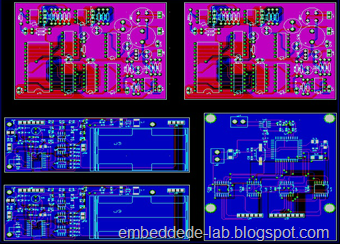
Merging different Prototype boards on a single Panel and generating Gerber Files for it, So that we can submit a single job to the PCB Manufacturer.
Note: This Tutorial applies only to double sided PCBs.
Contents
Introduction
Step 1 – Setting to Work
Step 2 - 4 – Viewing Gerber Files in Penalization mode
Step 5 – Arranging Boards on the Panel
Step 6 – Generate Gerber Files for the Panel
Conclusion
Introduction
Penalizing PCBs is the process of merging the Gerber files generated by a PCB package for different circuit boards in order to submit a single job to the PCB manufacturer. In this Tutorial we will merge Gerber files generated by Proteus ARES for three different boars. Proteus ARES generates Gerber files in RS-274X extended Gerber format. You can read about RS-274X and other Gerber formats at Wikipedia or somewhere else on the internet.
I assume you are familiar with schematic and PCB designing in the Proteus Design package. You can download the current free version of Proteus here. For this tutorial I used Version 7.7.
For this tutorial I am using three the Sample Project. I have previously generated the Gerber files for them in different folders for the sake of clarity
Project1-Gerber
Project2-Gerber
Project3-Gerber
Now we do the following steps to Panelize the Boards into a single Panel.
Step 1 - Setting to Work
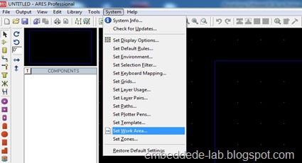
Open the Proteus ARES Program. Set the Work area to the size of the Panel. Here are some tips for selecting the size of the panel
- Know the dimensions of your boards
- How many copies of each board you want?
- What size Panel the PCB manufacturer can make(some PCB Manufacturers have restrictions on the Panel size some have not confirm it first).
- Select the Panel size so that you can optimally place your boards without wasting much space on the Panel.
Now you are ready to set the work area go to the windows menu and select the option “Set Work Area” enter the dimensions of the Panel and Hit Ok.

Step 2 – 4 – Viewing Gerber Files in Penalization mode
Step 2 -
Now it’s time to open all the Gerber File we have previously created in ARES. Click the Gerber Viewer icon in the toolbar or Find it in the Output drop-down menu, the Gerber View window appears, navigate to the project folder and open the GERBVIEW for the first project as shown in the figure.
Step 3 -
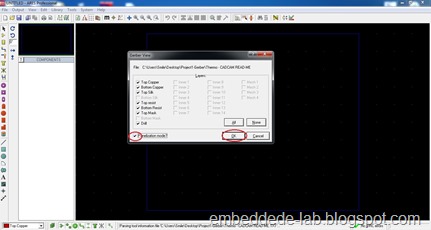
After clicking Open, In the next popup window don’t forget to check the option “Penalization mode” as shown. Click OK

We have just viewed Gerber Files for the First Project in ARES in Penalization mode.

Step 4 -
Follow step 2 to Step 3 for the other two boards.
Note: “Don’t move any of your board until you do the process for each board you want to be on the Panel”. If you move a board and then try to load another you will get the option to save your work, it doesn’t matter whether you save or not you will get the other board in new work area, which we don’t want here. So be careful
Step 5 – Arranging Boards on the Panel
Now that you have loaded all of your boards to the work area, it’s time to arrange them on the Panel.
If you want to make a copy of a board you simply select it right click and select “Block Copy” place it as many times you want and then click escape key to end.
I arranged the Boards as shown in the below image 
Step 6 – Generate Gerber Files for the Panel
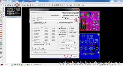
Now we have to generate Gerber files for the Panel which has our three Board on it, these are Gerber Files you will submit to the PCB Manufacturer. The Steps to generate and save the Gerber Files for the Panel are as below (in the image)
Conclusion
If you are having difficulty moving the boards, try to hide some layers.
This concludes the Tutorial.


Very interesting post. I like to share this post with my friends and book mark this interesting page. Keep it up..
ReplyDeleteSYS technologies Co., Ltd
You shared screenshots helped me a lot in my study, thanks for sharing. prototype pcb assembly
ReplyDeleteThat's what I needed. Thank you a lot!
ReplyDeleteThanks for Sharing such an informative content with us.
ReplyDeleteAlso Check: Study of PCB
Visit Website: EtoosIndia
This method won't pass the audit at the manufacturer. V-cuts or mouse bites are missing.
ReplyDeletethis blog is very nice circuit board design involves creating a layout for electronic components and conductive pathways on a PCB to ensure proper electrical connections and functionality.
ReplyDelete